A 300mm quantum wafer is not a finished quantum computer. It is the advanced manufacturing base on which quantum processor chips are built. That distinction matters because IBM’s Anderon foundry is not just another quantum announcement. It points to a deeper shift: quantum computing is moving from laboratory-built devices toward industrial chip manufacturing.
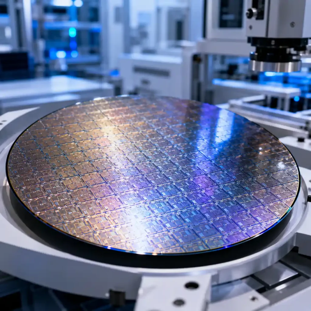
A 300mm wafer is a round silicon disc about 12 inches wide. In classical computing, companies use wafers to manufacture CPUs, GPUs and memory chips. In quantum computing, the same wafer-scale manufacturing idea is used to build the delicate structures that form quantum processors, including superconducting circuits, microwave wiring, resonators, couplers and control pathways.
The simplest real-world comparison is a bakery tray. A small tray lets a baker test a few pastries. A larger, standardized tray lets the bakery make more pastries, compare recipes faster and control quality better. A 300mm wafer works in a similar way for chipmakers. It gives engineers more surface area, more test structures and more design experiments on a single wafer.
Why 300mm matters for quantum chips
Quantum chips are extremely sensitive to tiny manufacturing differences. A small defect in metal thickness, surface contamination, wiring geometry or material interface can affect qubit performance. In superconducting quantum computers, qubits operate at temperatures close to absolute zero, and even microscopic imperfections can increase noise or shorten coherence time.
This is where 300mm fabrication becomes important. A modern 300mm fab uses highly automated semiconductor tools, advanced metrology and strict process control. That means engineers can measure, compare and improve chip quality across a full wafer instead of relying mainly on small experimental batches.
For example, if IBM tests ten different coupler designs or wiring layouts, a 300mm wafer can help place more variations on the same manufacturing run. Engineers can then compare which designs have lower loss, stronger connectivity or better uniformity. That shortens the learning cycle, which is critical because useful quantum computers will require better qubits, denser layouts and more reliable interconnects.
In simple terms: 300mm wafers help quantum companies move from “can we build one chip?” to “can we build many complex chips repeatedly, test them properly and improve them faster?”
The real technical advantage is not only wafer size. It is the manufacturing ecosystem around that size. A 300mm line can support cleaner deposition, tighter etching, better wafer inspection and more repeatable patterning. Those tools are already central to advanced semiconductor production, and quantum hardware now needs that same industrial discipline.
Quantum chips also face a packaging challenge. A processor must connect fragile qubits to control electronics through microwave signals without adding too much heat, noise or signal loss. Advanced wafer processing can support features such as through-silicon vias, bump bonding and multi-layer wiring, which are important as quantum processors become more complex.
That is why IBM’s Anderon foundry matters. It could provide a dedicated U.S. manufacturing base for quantum wafers rather than treating quantum chips as one-off research devices. IBM has already linked its 300mm quantum fabrication push to its broader quantum hardware roadmap, including more complex processors and faster development cycles through advanced semiconductor fabrication.
The real-world impact is easy to see. Drug discovery, battery chemistry, materials design and financial risk modelling are often mentioned as future quantum use cases. But none of those applications matter unless quantum machines can scale beyond fragile prototypes. Better wafers do not solve every quantum problem, but they attack one of the biggest bottlenecks: making quantum processors with enough quality, complexity and repeatability to keep improving.
IBM’s Anderon foundry therefore represents more than a new facility. It marks a point where quantum computing starts to resemble the chip industry: progress depends not only on physics breakthroughs, but also on factories, yield, process control and manufacturing scale.
Make Swikblog your go-to source on Google for reliable updates, smart insights, and daily trends.